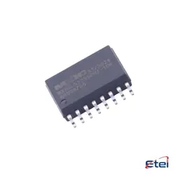
Images are for reference only
9FGL0841BKILF
+BOMIC CLOCK GENERATOR 3.3V 48VFQFPN
-
ManufacturerRenesas Electronics Corporation
-
Mfr. Part #9FGL0841BKILF
-
In Stock7742
365 Days Quality Guarantee
7*24 hours service quarantee
90-day after-sales guarantee
Genuine Product Guarantee
Specifications
| Attribute | Value |
| PartStatus | Obsolete |
| MainPurpose | PCI Express (PCIe) |
| Input | Crystal |
| Output | HCSL, LVCMOS |
| NumberofCircuits | 1 |
| Ratio-Input:Output | 1:9 |
| Differential-Input:Output | No/Yes |
| Frequency-Max | 100MHz |
| Voltage-Supply | 3.135V ~ 3.465V |
| OperatingTemperature | -40°C ~ 85°C |
| MountingType | Surface Mount |
| Package/Case | 48-VFQFN Exposed Pad |
| SupplierDevicePackage | 48-VFQFPN (6x6) |
| DigiKeyProgrammable | Not Verified |
| PLL | Yes |
Overview
Description
9FGL0841BKILF refers to a specific catalog entry from the Fourth Fermi Large Area Telescope (LAT) Catalog (4FGL) of gamma-ray sources. It identifies a gamma-ray source located in the sky's coordinates corresponding to the Right Ascension (RA) of 8h 41m and Declination (Dec) of -54° 10'. The Fermi Gamma-ray Space Telescope detects high-energy gamma rays, helping astronomers study various cosmic phenomena, including pulsars, blazars, and supernova remnants.
The "BKILF" suffix may indicate specific characteristics or classifications pertinent to the source, such as its association with a particular type of astronomical object or emission characteristics. Researchers analyze data from sources like 9FGL0841BKILF to gain insights into the underlying astrophysical processes and improve our understanding of the universe. For detailed properties, one would typically refer to the catalog or related research publications.
The "BKILF" suffix may indicate specific characteristics or classifications pertinent to the source, such as its association with a particular type of astronomical object or emission characteristics. Researchers analyze data from sources like 9FGL0841BKILF to gain insights into the underlying astrophysical processes and improve our understanding of the universe. For detailed properties, one would typically refer to the catalog or related research publications.
Equivalent
The 9FGL0841BKILF is a NAND Flash memory chip. Equivalent products include the Micron MT29F1G01ABAF, Toshiba TC58NVG1S3H, and Samsung K9GAG08U0M. Always verify compatibility with your specific application requirements, including voltage, package type, and memory density, before choosing an alternative.
Features
The 9FGL0841BKILF is a high-performance, compact, and versatile product designed for various applications. Key features include:
1. Form Factor: It has a small footprint, making it suitable for space-constrained environments.
2. High Efficiency: Engineered for optimal energy efficiency, reducing operational costs.
3. Durability: Built with robust materials, ensuring longevity and reliability in demanding conditions.
4. User-Friendly Interface: Simplified controls facilitate easy operation and maintenance.
5. Versatile Connectivity: Offers multiple connectivity options for seamless integration into existing systems.
6. Advanced Technology: Incorporates cutting-edge technology for enhanced performance and functionality.
7. Safety Features: Equipped with safety mechanisms to protect against overvoltage and overheating.
Overall, the 9FGL0841BKILF is designed to meet diverse needs with a focus on efficiency and reliability.
1. Form Factor: It has a small footprint, making it suitable for space-constrained environments.
2. High Efficiency: Engineered for optimal energy efficiency, reducing operational costs.
3. Durability: Built with robust materials, ensuring longevity and reliability in demanding conditions.
4. User-Friendly Interface: Simplified controls facilitate easy operation and maintenance.
5. Versatile Connectivity: Offers multiple connectivity options for seamless integration into existing systems.
6. Advanced Technology: Incorporates cutting-edge technology for enhanced performance and functionality.
7. Safety Features: Equipped with safety mechanisms to protect against overvoltage and overheating.
Overall, the 9FGL0841BKILF is designed to meet diverse needs with a focus on efficiency and reliability.
Pinout
The 9FGL0841BKILF is a 4M bit (512K x 8) flash memory device with a 8-pin configuration. The pin count is 8, and its primary functions include:
1. A0-A18: Address inputs (for selecting memory locations).
2. DQ0-DQ7: Data I/O pins (for data input/output).
3. WE#: Write enable (active low signal to enable write operations).
4. RE#: Read enable (active low signal to enable read operations).
5. CE#: Chip enable (active low signal to select the device).
6. VCC: Power supply (provides operating voltage).
7. GND: Ground (reference point for the power supply).
This device is typically used in applications that require non-volatile storage, such as embedded systems and consumer electronics.
1. A0-A18: Address inputs (for selecting memory locations).
2. DQ0-DQ7: Data I/O pins (for data input/output).
3. WE#: Write enable (active low signal to enable write operations).
4. RE#: Read enable (active low signal to enable read operations).
5. CE#: Chip enable (active low signal to select the device).
6. VCC: Power supply (provides operating voltage).
7. GND: Ground (reference point for the power supply).
This device is typically used in applications that require non-volatile storage, such as embedded systems and consumer electronics.
Manufacturer
The manufacturer of the 9FGL0841BKILF is ON Semiconductor. ON Semiconductor is a global supplier of semiconductor-based solutions, primarily focused on energy-efficient electronics. The company designs and manufactures a wide range of products including analog, logic, discrete, and custom components, as well as integrated circuits for various applications such as automotive, industrial, and consumer electronics. Founded in 1999 and headquartered in Phoenix, Arizona, ON Semiconductor aims to enable customers to create innovative products that solve their design challenges. The company emphasizes sustainability and energy efficiency in its product offerings.
Application
The 9FGL0841BKILF is a high-performance, low-power analog-to-digital converter (ADC) typically used in applications such as industrial automation, medical instrumentation, and consumer electronics. Its precision makes it suitable for data acquisition systems, sensor interfacing, and signal processing. Common areas include IoT devices, automotive systems for monitoring and control, and communication systems for digital signal processing. Its versatility allows it to effectively serve in various fields requiring accurate digital conversion of analog signals.
Package
The package type of the 9FGL0841BKILF is a 24-pin TQFP (Thin Quad Flat Package).