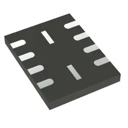
Images are for reference only
AOD413A
+BOMMOSFET P-CH 40V 12A TO252
-
ManufacturerAlpha & Omega Semiconductor Inc.
-
Mfr. Part #AOD413A
-
Datasheet AOD413A DataSheet
-
Package TO-252-3
-
In Stock3374
365 Days Quality Guarantee
7*24 hours service quarantee
90-day after-sales guarantee
Genuine Product Guarantee
Specifications
| Attribute | Value |
| Package / Case | Tape & Reel (TR),Cut Tape (CT) |
| Part Status | Active |
| FET Type | P-Channel |
| Technology | MOSFET (Metal Oxide) |
| Drain to Source Voltage (Vdss) | 40 V |
| Current - Continuous Drain(Id) @ 25°C | 12A (Tc) |
| Drive Voltage(Max Rds On Min Rds On) | 4.5V, 10V |
| Rds On(Max) @ Id Vgs | 44mOhm @ 12A, 10V |
| Vgs(th)(Max) @ Id | 3V @ 250µA |
| Gate Charge(Qg)(Max) @ Vgs | 21 nC @ 10 V |
| Vgs(Max) | ±20V |
| Input Capacitance(Ciss)(Max) @ Vds | 1125 pF @ 20 V |
| Power Dissipation (Max) | 2.5W (Ta), 50W (Tc) |
| Operating Temperature | -55°C ~ 175°C (TJ) |
| Mounting Type | Surface Mount |
| Supplier Device Package | TO-252 (DPAK) |
Overview
Description
- Voltage Rating: -30V
- Current Rating: -13A (continuous)
- Low On-Resistance (RDS(on)): 36mΩ (max at VGS = -10V)
- Fast Switching: Suitable for DC-DC converters, load switches, and battery protection.
- Compact Package: TO-252 (DPAK) for efficient PCB mounting.
It is commonly used in power supplies, motor control, and portable electronics due to its high efficiency and thermal performance. Always refer to the datasheet for detailed specifications and application guidelines.
Features
- Voltage Rating: -30V (Drain-to-Source, VDS)
- Current Rating: -8.7A (Continuous Drain Current, ID)
- Low On-Resistance: 36mΩ (at VGS = -10V)
- Fast Switching: Low gate charge (Qg = 13nC) for efficient performance
- Power Dissipation: 2.5W (TA = 25°C)
- Logic-Level Gate Drive: Fully enhanced at VGS = -4.5V
- Package: TO-252 (DPAK), surface-mountable
Ideal for power management, load switching, and DC-DC conversion in compact designs.
Pinout
Pin Functions:
1. Gate (G): Controls the MOSFET's switching.
2. Drain (D): Connects to the load (high-side switching).
3. Source (S): Connects to the power supply (typically V+).
Key Features:
- -30V drain-source voltage (VDS)
- -13A continuous drain current (ID)
- Low RDS(on) (e.g., ~40mΩ at VGS = -10V)
Used in power management, load switching, and DC-DC converters.
Application
1. Power Management – Voltage regulation, load switching in DC-DC converters.
2. Battery Protection – Reverse polarity and overcurrent protection in portable devices.
3. Motor Control – Driving small motors in automotive and industrial systems.
4. LED Drivers – Efficient power control in lighting applications.
5. Consumer Electronics – Power switching in laptops, smartphones, and power tools.
Its low on-resistance (RDS(on)) and high current handling (up to 13A) make it suitable for high-efficiency, compact designs.