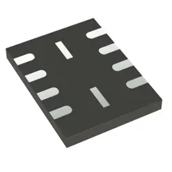
Images are for reference only
AON6240
+BOMMOSFET N-CH 40V 27A/85A 8DFN
-
ManufacturerAlpha & Omega Semiconductor Inc.
-
Mfr. Part #AON6240
-
Datasheet AON6240 DataSheet
-
In Stock5190
365 Days Quality Guarantee
7*24 hours service quarantee
90-day after-sales guarantee
Genuine Product Guarantee
Specifications
| Attribute | Value |
| Supplier | Alpha & Omega Semiconductor Inc. |
| Package / Case | Tape & Reel (TR),Cut Tape (CT) |
| Part Status | Not For New Designs |
| FET Type | N-Channel |
| Technology | MOSFET (Metal Oxide) |
| Drain to Source Voltage (Vdss) | 40 V |
| Current - Continuous Drain(Id) @ 25°C | 27A (Ta), 85A (Tc) |
| Drive Voltage(Max Rds On Min Rds On) | 4.5V, 10V |
| Rds On(Max) @ Id Vgs | 1.6mOhm @ 20A, 10V |
| Vgs(th)(Max) @ Id | 2.4V @ 250µA |
| Gate Charge(Qg)(Max) @ Vgs | 88 nC @ 10 V |
| Vgs(Max) | ±20V |
| Input Capacitance(Ciss)(Max) @ Vds | 6550 pF @ 20 V |
| Power Dissipation (Max) | 2.3W (Ta), 83W (Tc) |
| Operating Temperature | -55°C ~ 150°C (TJ) |
| Mounting Type | Surface Mount |
| Supplier Device Package | 8-DFN (5x6) |
Overview
Description
The introduction would set the stage for deeper exploration of these topics, providing students with essential background knowledge and preparing them for more complex concepts covered later in the course. Students might engage with lectures, hands-on projects, and case studies to gain practical experience. For specific details, including course objectives, prerequisites, or the exact curriculum, students should refer to the course syllabus or contact the instructor or academic department offering AON6240.
Equivalent
Features
1. N-Channel MOSFET: Designed for efficient switching applications.
2. Voltage Rating: Typically has a 30V maximum drain-source voltage (V_DS).
3. Current Handling: Capable of handling around 16A continuous drain current (I_D) under specific conditions.
4. Low On-Resistance: Features a low R_DS(on) value, enhancing efficiency by reducing power loss during operation.
5. Package Type: Often available in a compact DFN package (Dual Flat No-leads) for space-saving on printed circuit boards.
6. Thermal Performance: Designed for optimal thermal management, suitable for high-efficiency systems.
7. Applications: Commonly used in DC-DC converters, load switches, and other power management applications.
These features make the AON6240 a suitable choice for designers looking for compact and efficient power management solutions in various electronic applications.
Pinout
1. Pin 1 (G1): Gate of the first MOSFET.
2. Pin 2 (S1): Source of the first MOSFET.
3. Pin 3 (D1): Drain of the first MOSFET, commonly connected to the drain of the second MOSFET inside the package.
4. Pin 4 (D2): Drain of the second MOSFET, commonly connected to the drain of the first MOSFET inside the package.
5. Pin 5 (S2): Source of the second MOSFET.
6. Pin 6 (G2): Gate of the second MOSFET.
The AON6240 is used in applications requiring efficient switching and amplification in electronic circuits. Always refer to the specific datasheet for detailed and exact specifications, as variations can exist based on manufacturer updates or specific model versions.