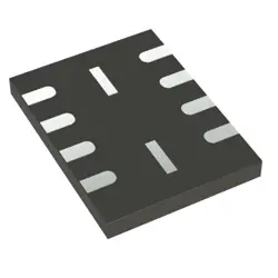
Images are for reference only
BD9G341AEFJ-LBE2
+BOMIC REG BUCK ADJ 3A 8HTSOP-J
-
ManufacturerRohm Semiconductor
-
Mfr. Part #BD9G341AEFJ-LBE2
-
In Stock7201
365 Days Quality Guarantee
7*24 hours service quarantee
90-day after-sales guarantee
Genuine Product Guarantee
Specifications
| Attribute | Value |
| Part Status | Active |
| Function | Step-Down |
| Output Configuration | Positive |
| Topology | Buck |
| Output Type | Adjustable |
| Number of Outputs | 1 |
| Voltage - Input (Min) | 12V |
| Voltage - Input (Max) | 76V |
| Voltage - Output (Min / Fixed) | 1V |
| Voltage - Output (Max) | 76V |
| Current - Output | 3A |
| Frequency - Switching | 50kHz ~ 750kHz |
| Synchronous Rectifier | No |
| Operating Temperature | -40°C ~ 85°C (TA) |
| Mounting Type | Surface Mount |
| Package / Case | 8-SOIC (0.154", 3.90mm Width) Exposed Pad |
| Supplier Device Package | 8-HTSOP-J |
| Base Product Number | BD9G341 |
Overview
Description
The BD9G341AEFJ-LBE2 is a step-down DC-DC converter from ROHM Semiconductor, known for its high-efficiency power management capabilities. It is designed to convert higher input voltages to lower output voltages efficiently, making it ideal for use in various electronic applications, such as communication devices, industrial equipment, and consumer electronics.
Key features of the BD9G341AEFJ-LBE2 include its wide input voltage range, typically from 4.5V to 42V, and an adjustable output voltage range, which provides flexibility in multiple application scenarios. The device supports a maximum output current of up to 3A and operates at a high switching frequency, which reduces the size of external components required and improves overall efficiency.
The converter also integrates protection features such as overcurrent protection, thermal shutdown, and undervoltage lockout, enhancing reliability and safety in end applications. Its compact HTSOP-J8 package allows for space-saving designs, making it suitable for compact, high-performance power supply solutions.
Key features of the BD9G341AEFJ-LBE2 include its wide input voltage range, typically from 4.5V to 42V, and an adjustable output voltage range, which provides flexibility in multiple application scenarios. The device supports a maximum output current of up to 3A and operates at a high switching frequency, which reduces the size of external components required and improves overall efficiency.
The converter also integrates protection features such as overcurrent protection, thermal shutdown, and undervoltage lockout, enhancing reliability and safety in end applications. Its compact HTSOP-J8 package allows for space-saving designs, making it suitable for compact, high-performance power supply solutions.
Equivalent
The BD9G341AEFJ-LBE2 is a DC-DC buck converter. Equivalent products might include similar buck converters from other manufacturers such as the LM2596 series from Texas Instruments, the NCP3063 from ON Semiconductor, or the MP1584 from Monolithic Power Systems. Ensure to compare specific parameters like input voltage range, output current, switching frequency, and efficiency to find a suitable match.
Features
The BD9G341AEFJ-LBE2 is a step-down switching regulator IC from Rohm Semiconductor. It features a wide input voltage range, typically from 4.5V to 42V, making it suitable for various industrial and automotive applications. The device provides a fixed output voltage, often around 3.3V or 5V, with a maximum output current capacity of around 0.5A to 1A, depending on external components and configuration.
Key features include high efficiency due to low RDS(ON) MOSFETs, and a switching frequency of approximately 2.2 MHz, which reduces the size of external components. The IC offers overcurrent protection, thermal shutdown, and undervoltage lockout (UVLO) to enhance reliability and safety. It supports a fast transient response and has a soft-start function to prevent inrush current during power-up.
The device typically comes in a compact and thermally efficient package, such as HTSOP-J8, making it suitable for space-constrained designs. Its robustness and efficiency make it ideal for power management in automotive and industrial applications.
Key features include high efficiency due to low RDS(ON) MOSFETs, and a switching frequency of approximately 2.2 MHz, which reduces the size of external components. The IC offers overcurrent protection, thermal shutdown, and undervoltage lockout (UVLO) to enhance reliability and safety. It supports a fast transient response and has a soft-start function to prevent inrush current during power-up.
The device typically comes in a compact and thermally efficient package, such as HTSOP-J8, making it suitable for space-constrained designs. Its robustness and efficiency make it ideal for power management in automotive and industrial applications.
Pinout
The BD9G341AEFJ-LBE2 is a DC-DC buck converter IC designed by ROHM Semiconductor. It is primarily used for step-down power conversion in electronic devices. The IC comes in a 8-pin HTSOP-J8 package. The functions of these pins are:
1. VIN (Pin 1): Input voltage supply pin.
2. SW (Pin 2): Switch pin connected to the inductor.
3. GND (Pin 3): Ground pin for the IC.
4. FB (Pin 4): Feedback pin for voltage regulation.
5. COMP (Pin 5): Compensation pin for stabilizing the control loop.
6. EN (Pin 6): Enable pin to turn the IC on or off.
7. RT (Pin 7): Timing resistor pin to set the switching frequency.
8. VCC (Pin 8): Output of the internal regulator, typically used for internal circuitry.
The BD9G341AEFJ-LBE2 is used for efficient power management in various applications, providing a stable output voltage from a higher input voltage.
1. VIN (Pin 1): Input voltage supply pin.
2. SW (Pin 2): Switch pin connected to the inductor.
3. GND (Pin 3): Ground pin for the IC.
4. FB (Pin 4): Feedback pin for voltage regulation.
5. COMP (Pin 5): Compensation pin for stabilizing the control loop.
6. EN (Pin 6): Enable pin to turn the IC on or off.
7. RT (Pin 7): Timing resistor pin to set the switching frequency.
8. VCC (Pin 8): Output of the internal regulator, typically used for internal circuitry.
The BD9G341AEFJ-LBE2 is used for efficient power management in various applications, providing a stable output voltage from a higher input voltage.
Manufacturer
The BD9G341AEFJ-LBE2 is manufactured by ROHM Semiconductor. ROHM is a Japanese company that specializes in the design and manufacturing of electronic components, including semiconductors, integrated circuits, and other electronic devices. The company was founded in 1958 and has since grown into a global enterprise. ROHM is known for its high-quality products and innovative solutions, serving a wide range of industries such as automotive, consumer electronics, telecommunications, and industrial equipment. The company focuses on developing advanced technologies to meet the needs of its diverse clientele and is recognized for its contributions to the electronics industry.
Application
The BD9G341AEFJ-LBE2 is typically used in power management applications. It is suitable for use in DC-DC converters, specifically step-down (buck) converter circuits. Its applications include powering microcontrollers, FPGAs, ASICs, and similar digital components in consumer electronics, industrial equipment, communication devices, and automotive systems. Its high efficiency and compact size make it ideal for battery-powered devices and space-constrained applications.
Package
The BD9G341AEFJ-LBE2 is a buck converter IC from ROHM Semiconductor, typically used for efficient voltage regulation. It comes in a compact HTSOP-J8 package, which is a Heat Sink Thin Shrink Outline Package with 8 pins, designed for surface mounting. This package type helps with efficient heat dissipation, making it suitable for power applications.