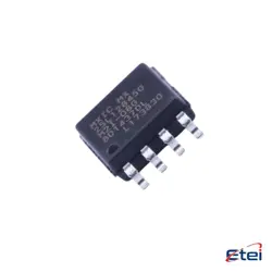
Images are for reference only
GD25LD40CEIGR
+BOMIC FLSH 4MBIT SPI/DUAL I/O 8USON
-
ManufacturerGigaDevice Semiconductor (HK) Limited
-
Mfr. Part #GD25LD40CEIGR
-
In Stock3103
365 Days Quality Guarantee
7*24 hours service quarantee
90-day after-sales guarantee
Genuine Product Guarantee
Specifications
| Attribute | Value |
| Part Status | Active |
| Digi Key Programmable | Not Verified |
| Memory Type | Non-Volatile |
| Memory Format | FLASH |
| Technology | FLASH - NOR |
| Memory Size | 4Mbit |
| Memory Organization | 512K x 8 |
| Memory Interface | SPI - Dual I/O |
| Clock Frequency | 50 MHz |
| Write Cycle Time - Word, Page | 97µs, 6ms |
| Voltage - Supply | 1.65V ~ 2V |
| Operating Temperature | -40°C ~ 85°C (TA) |
| Mounting Type | Surface Mount |
| Package / Case | 8-XFDFN Exposed Pad |
| Supplier Device Package | 8-USON (2x3) |
| Base Product Number | GD25LD40 |
Overview
Description
The GD25LD40CEIGR is a 4 Megabit (512 Kbyte) serial NOR Flash memory manufactured by GigaDevice. It features a high-speed SPI (Serial Peripheral Interface) that supports data rates up to 104 MHz, optimizing performance for applications requiring fast data access. The device operates on a voltage range of 2.7V to 3.6V and supports a wide temperature range, making it suitable for various environments.
Key features include support for dual and quad SPI modes, allowing increased data transfer rates, and it is designed to efficiently execute erase, program, and read operations. The GD25LD40CEIGR is commonly used in consumer electronics, automotive, and industrial applications for code storage, firmware updates, and more due to its reliability and flexibility. The package comes in a compact 8-pin SOIC, facilitating easy integration into designs. Overall, it is ideal for applications that require non-volatile memory with high-speed access, low power consumption, and robust performance.
Key features include support for dual and quad SPI modes, allowing increased data transfer rates, and it is designed to efficiently execute erase, program, and read operations. The GD25LD40CEIGR is commonly used in consumer electronics, automotive, and industrial applications for code storage, firmware updates, and more due to its reliability and flexibility. The package comes in a compact 8-pin SOIC, facilitating easy integration into designs. Overall, it is ideal for applications that require non-volatile memory with high-speed access, low power consumption, and robust performance.
Equivalent
The GD25LD40CEIGR chip is a 4Mb NOR Flash memory. Equivalent products include:
1. Winbond W25Q40BV
2. Micron MT25QL040A
3. Spansion S25FL040A
4. Cypress S25FL040K
These alternatives provide similar specifications regarding capacity, voltage, and interfaces, making them suitable replacements in most applications. Always check the datasheets for compatibility.
1. Winbond W25Q40BV
2. Micron MT25QL040A
3. Spansion S25FL040A
4. Cypress S25FL040K
These alternatives provide similar specifications regarding capacity, voltage, and interfaces, making them suitable replacements in most applications. Always check the datasheets for compatibility.
Features
The GD25LD40CEIGR is a 4 Mbit (512 K x 8) Serial Flash memory device from GigaDevice. Key features include:
1. Interface: It supports a quad SPI (Serial Peripheral Interface) protocol for high-speed data transfer.
2. Operating Voltage: The device operates at a voltage range of 2.7V to 3.6V.
3. Speed: It offers up to 104 MHz clock frequency for efficient data access.
4. Memory Organization: The memory is organized into 256 sectors of 64 Kbits each, allowing for flexible data management.
5. Erase and Programming: Supports sector erase, bulk erase, and page programming capabilities.
6. Endurance: The device has a typical endurance of 100,000 program/erase cycles per sector.
7. Data Retention: Offers a data retention period of up to 20 years.
8. Package Options: Available in various package types, including SOIC and WSON.
These features make the GD25LD40CEIGR suitable for applications in consumer electronics, automotive, and industrial sectors.
1. Interface: It supports a quad SPI (Serial Peripheral Interface) protocol for high-speed data transfer.
2. Operating Voltage: The device operates at a voltage range of 2.7V to 3.6V.
3. Speed: It offers up to 104 MHz clock frequency for efficient data access.
4. Memory Organization: The memory is organized into 256 sectors of 64 Kbits each, allowing for flexible data management.
5. Erase and Programming: Supports sector erase, bulk erase, and page programming capabilities.
6. Endurance: The device has a typical endurance of 100,000 program/erase cycles per sector.
7. Data Retention: Offers a data retention period of up to 20 years.
8. Package Options: Available in various package types, including SOIC and WSON.
These features make the GD25LD40CEIGR suitable for applications in consumer electronics, automotive, and industrial sectors.
Pinout
The GD25LD40CEIGR is a 4 Mbit (512 K x 8) Serial NOR Flash memory device. It typically comes in an 8-pin SOIC package. The pin count and functions are as follows:
1. CS (Chip Select): Active low input for selecting the device.
2. SO (Serial Output): Output pin for data.
3. SI (Serial Input): Input pin for data.
4. SCK (Serial Clock): Clock input pin for synchronizing data transfer.
5. GND (Ground): Power ground pin.
6. VCC (Power Supply): Supply voltage pin, typically 2.7V to 3.6V.
7. WP (Write Protect): Input pin to protect memory from write operations (active high).
8. HOLD: Input pin to pause the serial communication (active low).
This device supports various serial communication protocols, including SPI, and is used in various applications requiring non-volatile memory.
1. CS (Chip Select): Active low input for selecting the device.
2. SO (Serial Output): Output pin for data.
3. SI (Serial Input): Input pin for data.
4. SCK (Serial Clock): Clock input pin for synchronizing data transfer.
5. GND (Ground): Power ground pin.
6. VCC (Power Supply): Supply voltage pin, typically 2.7V to 3.6V.
7. WP (Write Protect): Input pin to protect memory from write operations (active high).
8. HOLD: Input pin to pause the serial communication (active low).
This device supports various serial communication protocols, including SPI, and is used in various applications requiring non-volatile memory.
Manufacturer
The manufacturer of the GD25LD40CEIGR is GigaDevice Semiconductor Inc. GigaDevice is a Chinese company that specializes in the design and production of semiconductor devices, primarily focused on memory solutions such as flash memory, including NOR Flash, NAND Flash, and DRAM. Established in 2005, the company has developed a reputation for its innovative memory products tailored for various applications, including consumer electronics, automotive, industrial, and Internet of Things (IoT) devices.
The GD25LD40CEIGR is a 4 Megabit (512 K x 8) Serial NOR Flash memory device, primarily used for code storage and execution in embedded systems. GigaDevice emphasizes high performance, reliability, and low power consumption in its product offerings, catering to the growing demand for memory solutions in the rapidly evolving tech landscape. The company operates in a competitive semiconductor market and seeks to provide advanced memory technologies to meet the needs of its diverse clientele.
The GD25LD40CEIGR is a 4 Megabit (512 K x 8) Serial NOR Flash memory device, primarily used for code storage and execution in embedded systems. GigaDevice emphasizes high performance, reliability, and low power consumption in its product offerings, catering to the growing demand for memory solutions in the rapidly evolving tech landscape. The company operates in a competitive semiconductor market and seeks to provide advanced memory technologies to meet the needs of its diverse clientele.
Application
The GD25LD40CEIGR is a 4 Mbit serial NOR Flash memory, commonly used in embedded systems. Its application areas include firmware storage for microcontrollers, data logging in industrial devices, boot code storage in consumer electronics, and configuration settings in automotive systems. It is also utilized in Internet of Things (IoT) devices for storing application code and user data. Its fast read speeds and reliable performance make it suitable for applications requiring quick access to stored data.
Package
The GD25LD40CEIGR is typically packaged in an 8-pin SOIC (Small Outline Integrated Circuit) package. This package type is commonly used for flash memory devices and allows for efficient surface mounting on PCBs.