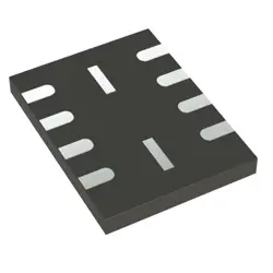
Images are for reference only
HEF4538BT
+BOMMonostable Multivibrator
-
ManufacturerNexperia
-
Mfr. Part #HEF4538BT
-
In Stock4219
365 Days Quality Guarantee
7*24 hours service quarantee
90-day after-sales guarantee
Genuine Product Guarantee
Specifications
| Attribute | Value |
Overview
Description
The HEF4538BT is a dual monostable multivibrator integrated circuit, commonly used in digital electronics for generating precise time delays or pulse width modulation. It is part of the 4000 series of ICs, which are known for their versatility and compatibility with CMOS technology. The HEF4538BT features two independent monostable multivibrators, each triggered by either a positive or negative edge. These circuits can be used to create timing applications such as debounce circuits, pulse generation, and delay timers.
Key features include:
- Dual monostable operation.
- Retriggerable capability, allowing for pulse extension.
- Wide operating voltage range from 3V to 15V.
- Low power consumption, typical of CMOS technology.
- Adjustable output pulse width via external resistor and capacitor.
The device is encapsulated in a 16-pin dual in-line package (DIP), making it easy to integrate into various designs. It is widely used in applications requiring digital timing solutions, thanks to its reliability and ease of use.
Key features include:
- Dual monostable operation.
- Retriggerable capability, allowing for pulse extension.
- Wide operating voltage range from 3V to 15V.
- Low power consumption, typical of CMOS technology.
- Adjustable output pulse width via external resistor and capacitor.
The device is encapsulated in a 16-pin dual in-line package (DIP), making it easy to integrate into various designs. It is widely used in applications requiring digital timing solutions, thanks to its reliability and ease of use.
Equivalent
The HEF4538BT is a dual monostable multivibrator IC. Equivalent products include the CD4538B from Texas Instruments, MC14538B from ON Semiconductor, and NTE4538B from NTE Electronics. These ICs typically offer similar functionality and pin configurations, making them suitable replacements in various applications. Always consult the datasheet to ensure full compatibility.
Features
The HEF4538BT is a dual monostable multivibrator integrated circuit, notable for its precision and reliability in timing applications. Key features include:
1. Dual Monostable Multivibrators: It contains two independent monostable multivibrators, each with its own control inputs and outputs.
2. Wide Supply Voltage Range: Operates efficiently over a supply voltage range from 3V to 15V, offering flexibility for various applications.
3. Triggering: Features both positive and negative edge-triggered inputs, allowing it to react to different types of input signals.
4. Schmitt-Trigger Action: Provides noise immunity on the trigger inputs, ensuring stable and reliable operation in noisy environments.
5. Long Timing Periods: Capable of generating long timing intervals using external resistors and capacitors.
6. Low Power Consumption: Designed for minimal power usage, making it suitable for battery-powered devices.
7. Temperature Range: Operates over a broad temperature range, enhancing its suitability for diverse environmental conditions.
These features make the HEF4538BT ideal for use in pulse generation, timing delay, and signal timing applications.
1. Dual Monostable Multivibrators: It contains two independent monostable multivibrators, each with its own control inputs and outputs.
2. Wide Supply Voltage Range: Operates efficiently over a supply voltage range from 3V to 15V, offering flexibility for various applications.
3. Triggering: Features both positive and negative edge-triggered inputs, allowing it to react to different types of input signals.
4. Schmitt-Trigger Action: Provides noise immunity on the trigger inputs, ensuring stable and reliable operation in noisy environments.
5. Long Timing Periods: Capable of generating long timing intervals using external resistors and capacitors.
6. Low Power Consumption: Designed for minimal power usage, making it suitable for battery-powered devices.
7. Temperature Range: Operates over a broad temperature range, enhancing its suitability for diverse environmental conditions.
These features make the HEF4538BT ideal for use in pulse generation, timing delay, and signal timing applications.
Pinout
The HEF4538BT is a dual monostable multivibrator integrated circuit. It features a total of 16 pins. The device is used to generate precise time delays or pulse widths and operates over a wide range of supply voltages.
Here's a brief description of the pin configuration and functions:
1. Pin 1 (A1): Input for the first monostable.
2. Pin 2 (B1): Second input for the first monostable.
3. Pin 3 (Q1): Output for the first monostable.
4. Pin 4 (Q1): Complementary output for the first monostable.
5. Pin 5 (Cext1): External capacitor connection for the first monostable.
6. Pin 6 (Rext1): External resistor connection for the first monostable.
7. Pin 7 (Cext2): External capacitor connection for the second monostable.
8. Pin 8 (Rext2): External resistor connection for the second monostable.
9. Pin 9 (Q2): Complementary output for the second monostable.
10. Pin 10 (Q2): Output for the second monostable.
11. Pin 11 (B2): Second input for the second monostable.
12. Pin 12 (A2): Input for the second monostable.
13. Pin 13 (VSS): Ground connection.
14. Pin 14 (VDD): Positive supply voltage connection.
15. Pin 15 (RESET1): Reset input for the first monostable.
16. Pin 16 (RESET2): Reset input for the second monostable.
This IC is typically used in timing applications, where precise control over pulse width is needed.
Here's a brief description of the pin configuration and functions:
1. Pin 1 (A1): Input for the first monostable.
2. Pin 2 (B1): Second input for the first monostable.
3. Pin 3 (Q1): Output for the first monostable.
4. Pin 4 (Q1): Complementary output for the first monostable.
5. Pin 5 (Cext1): External capacitor connection for the first monostable.
6. Pin 6 (Rext1): External resistor connection for the first monostable.
7. Pin 7 (Cext2): External capacitor connection for the second monostable.
8. Pin 8 (Rext2): External resistor connection for the second monostable.
9. Pin 9 (Q2): Complementary output for the second monostable.
10. Pin 10 (Q2): Output for the second monostable.
11. Pin 11 (B2): Second input for the second monostable.
12. Pin 12 (A2): Input for the second monostable.
13. Pin 13 (VSS): Ground connection.
14. Pin 14 (VDD): Positive supply voltage connection.
15. Pin 15 (RESET1): Reset input for the first monostable.
16. Pin 16 (RESET2): Reset input for the second monostable.
This IC is typically used in timing applications, where precise control over pulse width is needed.
Manufacturer
The HEF4538BT is manufactured by Nexperia. Nexperia is a global semiconductor company that specializes in producing discrete, logic, and MOSFET devices. The company was originally part of NXP Semiconductors but became an independent entity in 2017 when it was acquired by a consortium of investors led by Beijing Jianguang Asset Management and Wise Road Capital. Nexperia focuses on delivering high-volume, high-efficiency semiconductor components that are essential in various applications, including automotive, industrial, computing, and consumer electronics.
Application
The HEF4538BT is a dual monostable multivibrator integrated circuit commonly used in electronic applications requiring precise timing and pulse generation. Key application areas include:
1. Timing and Delay Generation: Used in circuits where specific timing delays are needed.
2. Pulse Shaping: Converts irregular, noisy signals into clean, uniform pulse shapes.
3. Frequency Division: Helps in generating lower frequency signals from a higher frequency source.
4. Debouncing: Eliminates noise in mechanical switches, ensuring clean digital signals.
5. Oscillator Circuits: Serves as a basic oscillator for generating clock signals.
6. Signal Conditioning: Adjusts signal characteristics for further processing or interfacing.
These features make it suitable for use in consumer electronics, communication systems, and industrial control applications.
1. Timing and Delay Generation: Used in circuits where specific timing delays are needed.
2. Pulse Shaping: Converts irregular, noisy signals into clean, uniform pulse shapes.
3. Frequency Division: Helps in generating lower frequency signals from a higher frequency source.
4. Debouncing: Eliminates noise in mechanical switches, ensuring clean digital signals.
5. Oscillator Circuits: Serves as a basic oscillator for generating clock signals.
6. Signal Conditioning: Adjusts signal characteristics for further processing or interfacing.
These features make it suitable for use in consumer electronics, communication systems, and industrial control applications.
Package
The HEF4538BT is a dual monostable multivibrator integrated circuit. It is typically available in a surface mount package known as SO16, which is a Small Outline package with 16 pins.