
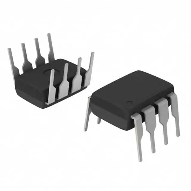
Images are for reference only
L6565N
+BOMIC OFFLINE SWITCH FLYBACK 8DIP
-
ManufacturerSTMicroelectronics
-
Mfr. Part #L6565N
-
Datasheet L6565N DataSheet
-
In Stock7627
365 Days Quality Guarantee
7*24 hours service quarantee
90-day after-sales guarantee
Genuine Product Guarantee
Specifications
| Attribute | Value |
| Part Status | Active |
| Output Isolation | Isolated |
| Internal Switch(s) | No |
| Topology | Flyback |
| Voltage - Supply (Vcc/Vdd) | 10.3V ~ 18V |
| Fault Protection | Current Limiting |
| Operating Temperature | -40°C ~ 150°C (TJ) |
| Package / Case | 8-DIP (0.300", 7.62mm) |
| Supplier Device Package | 8-DIP |
| Mounting Type | Through Hole |
| Base Product Number | L6565 |
| Voltage - Start Up | 13.5 V |
Overview
Description
Equivalent
1. UC3842 - A widely used PWM controller with similar functionalities.
2. NCP1200 - A PWM controller from ON Semiconductor.
3. SG6848 - A PWM controller for switch-mode power supplies.
4. FAN7554 - A Fairchild (now ON Semiconductor) controller IC.
These alternatives offer comparable features and functionalities for similar applications. Always check the datasheet for compatibility.
Features
1. Quasi-Resonant Operation: Enhances efficiency by reducing switching losses through zero-voltage switching.
2. Current-Mode Control: Provides superior regulation and fast transient response.
3. Integrated HV Startup: Simplifies circuit design and reduces power consumption during startup.
4. Low Standby Power: Designed to minimize power consumption in standby mode, making it suitable for energy-efficient applications.
5. Protection Features: Includes over-voltage, over-current, and thermal shutdown protection to ensure reliability and safety.
6. Frequency Modulation: Helps spread the frequency spectrum to reduce electromagnetic interference (EMI).
7. Adjustable Parameters: Offers flexibility through external components to tailor performance according to specific design needs.
8. Compact Package: Available in DIP-8 and SO-8 packages, making it suitable for space-constrained designs.
This IC is ideal for applications like power adapters, chargers, and small power supplies where efficiency and space are critical.
Pinout
1. VCC (Pin 1): Supply voltage for the IC.
2. GND (Pin 2): Ground reference for the IC.
3. COMP (Pin 3): Compensation for the feedback loop, connected to an external network to stabilize the converter.
4. CS (Pin 4): Current sense input for monitoring the current through the power switch.
5. ZCD (Pin 5): Zero Current Detection input to improve efficiency by detecting the zero current condition in the transformer.
6. OSC (Pin 6): Oscillator pin, used to set the switching frequency with external resistors and capacitors.
7. OUT (Pin 7): Output drive for the power MOSFET gate, controlled by the IC.
8. PWR (Pin 8): Power supply input for the IC, similar to VCC.
These pins collectively allow the L6565N to control the operation of resonant converters efficiently.
Manufacturer
Application
1. Switch Mode Power Supplies (SMPS): Enhancing efficiency and reducing input current distortion.
2. LED Drivers: Improving power factor and efficiency in LED lighting systems.
3. Industrial Power Systems: Ensuring compliance with power quality standards.
4. Consumer Electronics: Used in devices like TVs and computers to meet regulatory energy standards.
5. Telecom Power Supplies: Increasing efficiency and reliability in telecom infrastructure.
These applications benefit from the L6565N's ability to optimize power usage and reduce energy waste.


