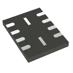
Images are for reference only
LTC6957IDD-2
+BOMIC CLK BUFFER 1:2 300MHZ 12DFN
-
ManufacturerAnalog Devices Inc.
-
Mfr. Part #LTC6957IDD-2
-
In Stock1469
365 Days Quality Guarantee
7*24 hours service quarantee
90-day after-sales guarantee
Genuine Product Guarantee
Specifications
| Attribute | Value |
| PartStatus | Obsolete |
| BaseProductNumber | LTC6957 |
| Type | Fanout Buffer (Distribution) |
| NumberofCircuits | 1 |
| Ratio-Input:Output | 1:2 |
| Differential-Input:Output | Yes/Yes |
| Input | CML, CMOS, LVDS, LVPECL |
| Output | LVDS |
| Frequency-Max | 300 MHz |
| Voltage-Supply | 3.15V ~ 3.45V |
| OperatingTemperature | -40°C ~ 85°C |
| MountingType | Surface Mount |
| Package | 12-WFDFN Exposed Pad |
| SupplierDevicePackage | 12-DFN (3x3) |
| Packaging | Tube |
Overview
Description
The LTC6957IDD-2 is a high-performance, low-jitter, dual-output clock buffer and distribution IC from Analog Devices. It is designed to distribute precision clock signals with minimal added phase noise or jitter, making it ideal for high-frequency applications such as communication systems, data converters, and other timing-sensitive electronic systems.
Key features include two independent, low-skew, low-noise outputs that can drive AC- or DC-coupled loads. The device operates with input frequencies up to 3 GHz and supports a wide supply voltage range, enhancing its versatility in various systems. Additionally, the LTC6957IDD-2 offers excellent power supply noise rejection and has a programmable output common mode voltage to ensure compatibility with different logic families.
Packaged in a compact, 10-lead DFN package, it is suitable for space-constrained applications. It is also notable for its low current consumption, which is beneficial in power-sensitive applications. The LTC6957IDD-2 serves as a reliable solution for distributing high-fidelity clock signals in demanding electronic environments.
Key features include two independent, low-skew, low-noise outputs that can drive AC- or DC-coupled loads. The device operates with input frequencies up to 3 GHz and supports a wide supply voltage range, enhancing its versatility in various systems. Additionally, the LTC6957IDD-2 offers excellent power supply noise rejection and has a programmable output common mode voltage to ensure compatibility with different logic families.
Packaged in a compact, 10-lead DFN package, it is suitable for space-constrained applications. It is also notable for its low current consumption, which is beneficial in power-sensitive applications. The LTC6957IDD-2 serves as a reliable solution for distributing high-fidelity clock signals in demanding electronic environments.
Equivalent
The LTC6957IDD-2 is a dual-channel, low-jitter, fanout buffer. Equivalent products may include:
1. ADCLK944 from Analog Devices: A low-jitter, dual-output buffer.
2. LMK1C110x series from Texas Instruments: Low-jitter, differential clock buffers.
3. Si533xx series from Silicon Labs: Low-phase-noise, low-jitter clock buffers.
4. NB3N2010 from ON Semiconductor: Precision clock buffer with low output skew.
Always verify the specific application requirements, as parameters like jitter, power supply, and temperature range may vary.
1. ADCLK944 from Analog Devices: A low-jitter, dual-output buffer.
2. LMK1C110x series from Texas Instruments: Low-jitter, differential clock buffers.
3. Si533xx series from Silicon Labs: Low-phase-noise, low-jitter clock buffers.
4. NB3N2010 from ON Semiconductor: Precision clock buffer with low output skew.
Always verify the specific application requirements, as parameters like jitter, power supply, and temperature range may vary.
Features
The LTC6957IDD-2 is a dual-output, low-noise, and low-jitter buffer designed for RF and high-speed digital systems. Key features include:
1. Ultra-Low Phase Noise and Jitter: It provides an exceptionally low additive phase noise of -162 dBc/Hz at 10 kHz offset and a jitter of 45 fs RMS.
2. High-Performance Outputs: The device features two independent, differential outputs, each capable of driving AC-coupled or DC-coupled loads.
3. Wide Frequency Range: It supports a wide input frequency range, typically from DC up to 3 GHz, making it versatile for various applications.
4. Low Power Consumption: The buffer operates with low power, requiring a single 3.3V supply.
5. Flexible Output Levels: It offers programmable output levels for both LVPECL and LVDS standards.
6. Enable Function: Each output channel has an independent enable pin for power management and system flexibility.
7. Compact Package: It is housed in a 4mm x 3mm QFN package, making it suitable for space-constrained designs.
These features make the LTC6957IDD-2 ideal for clock distribution in communication systems, data converters, and other precision timing applications.
1. Ultra-Low Phase Noise and Jitter: It provides an exceptionally low additive phase noise of -162 dBc/Hz at 10 kHz offset and a jitter of 45 fs RMS.
2. High-Performance Outputs: The device features two independent, differential outputs, each capable of driving AC-coupled or DC-coupled loads.
3. Wide Frequency Range: It supports a wide input frequency range, typically from DC up to 3 GHz, making it versatile for various applications.
4. Low Power Consumption: The buffer operates with low power, requiring a single 3.3V supply.
5. Flexible Output Levels: It offers programmable output levels for both LVPECL and LVDS standards.
6. Enable Function: Each output channel has an independent enable pin for power management and system flexibility.
7. Compact Package: It is housed in a 4mm x 3mm QFN package, making it suitable for space-constrained designs.
These features make the LTC6957IDD-2 ideal for clock distribution in communication systems, data converters, and other precision timing applications.
Pinout
The LTC6957IDD-2 is a dual-channel ultralow jitter buffer/driver IC. It comes in a 3mm × 3mm 10-lead DFN (Dual Flat No-Lead) package. The primary function of the LTC6957IDD-2 is to serve as a clock fan-out buffer, capable of distributing high-frequency clock signals with minimal jitter. The device is designed to drive 50-ohm transmission lines and is optimized for low additive phase noise performance, ensuring precision in frequency synthesis applications.
This IC is often used in applications requiring precise clock distribution, such as communication systems, data converters, and radar systems.
This IC is often used in applications requiring precise clock distribution, such as communication systems, data converters, and radar systems.
Manufacturer
The LTC6957IDD-2 is manufactured by Analog Devices, Inc. Analog Devices is a multinational semiconductor company that specializes in the design and manufacturing of analog, mixed-signal, and digital signal processing (DSP) integrated circuits. The company provides a wide range of products and solutions for various industries, including communications, automotive, industrial automation, healthcare, and consumer electronics. Analog Devices is known for its expertise in high-performance analog technology and innovation, offering products such as amplifiers, converters, power management ICs, sensors, and RF components.
Application
The LTC6957IDD-2 is a low-noise, low-jitter buffer/driver used in high-frequency applications. Key application areas include:
1. Communication Systems: It is used in clock distribution for telecom and networking systems, ensuring signal integrity.
2. Data Acquisition: Supports high-speed ADCs and DACs by providing precise clock signals.
3. Test and Measurement Equipment: Enhances the accuracy of frequency and time-domain measurements.
4. Radar and Satellite Systems: Used in signal processing chains where low phase noise is critical.
5. Wireless Infrastructure: Assists in maintaining synchronization in base stations and other wireless systems.
Its low additive jitter makes it suitable for high-performance, frequency-sensitive applications.
1. Communication Systems: It is used in clock distribution for telecom and networking systems, ensuring signal integrity.
2. Data Acquisition: Supports high-speed ADCs and DACs by providing precise clock signals.
3. Test and Measurement Equipment: Enhances the accuracy of frequency and time-domain measurements.
4. Radar and Satellite Systems: Used in signal processing chains where low phase noise is critical.
5. Wireless Infrastructure: Assists in maintaining synchronization in base stations and other wireless systems.
Its low additive jitter makes it suitable for high-performance, frequency-sensitive applications.
Package
The LTC6957IDD-2 is packaged in a 12-lead (3mm x 3mm) DFN (dual flat no-leads) package.