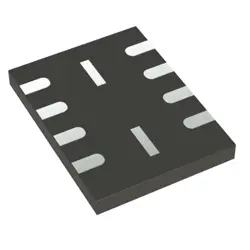
Images are for reference only
M24M01-DFMN6TP
+BOMIC EEPROM 1MBIT I2C 1MHZ 8SO
-
ManufacturerSTMicroelectronics
-
Mfr. Part #M24M01-DFMN6TP
-
Datasheet M24M01-DFMN6TP DataSheet
-
Package SO-8
-
In Stock3395
365 Days Quality Guarantee
7*24 hours service quarantee
90-day after-sales guarantee
Genuine Product Guarantee
Specifications
| Attribute | Value |
| Package / Case | Tape & Reel (TR),Cut Tape (CT) |
| Part Status | Active |
| Memory Type | Non-Volatile |
| Memory Format | EEPROM |
| Technology | EEPROM |
| Memory Size | 1Mb (128K x 8) |
| Memory Interface | I²C |
| Clock Frequency | 1 MHz |
| Write Cycle Time - Word Page | 5ms |
| Access Time | 500 ns |
| Voltage - Supply | 1.7V ~ 5.5V |
| Operating Temperature | -40°C ~ 85°C (TA) |
| Mounting Type | Surface Mount |
Overview
Description
Key features of the M24M01-DFMN6TP might include a 1 Mbit (128 Kbyte) storage capacity, organized as 131,072 x 8 bits. It typically supports I2C (Inter-Integrated Circuit) communication, which is a standard protocol for interfacing low-speed peripherals. The component is designed for high reliability, with the capability to perform a large number of write/erase cycles, and offers data retention for several decades.
The "DFMN6TP" part of the name refers to specific packaging and temperature specifications, indicating its suitability for various environmental conditions. The small form factor of its packaging suits applications where space is limited.
Equivalent
1. AT24CM01 from Microchip Technology
2. BR24G1MF from ROHM Semiconductor
3. FM24CL16B from Cypress Semiconductor (now Infineon Technologies)
Be sure to check specific electrical and performance characteristics to ensure compatibility in your application.
Features
1. Memory Capacity: 1 Mbit (128 Kbytes) organized as 128K x 8 bits, providing ample storage for various applications.
2. Interface: It utilizes an I²C (Inter-Integrated Circuit) interface, supporting fast-mode and fast-mode plus, with data transfer rates of up to 1 MHz.
3. Voltage Range: Operates over a supply voltage range of 1.8V to 5.5V, making it suitable for a wide range of applications and ensuring compatibility with different power sources.
4. Write Protection: Offers hardware write protection, which can be configured to protect the entire memory or partial areas from accidental writing, ensuring data integrity.
5. Endurance and Data Retention: Guarantees 1 million write cycles per byte and provides data retention for more than 40 years, ensuring long-term reliability.
6. Package: Available in a DFN (Dual Flat No-Lead) package, which is compact and suitable for space-constrained applications.
7. Applications: Used in consumer electronics, industrial systems, and other devices requiring non-volatile memory storage.
Pinout
1. VCC (Pin 1): Power supply pin.
2. A0, A1, A2 (Pins 2, 3, 4): Hardware address pins; used to configure the device's address.
3. VSS (Pin 5): Ground connection.
4. SDA (Pin 6): Serial Data; a bidirectional line for data transfer.
5. SCL (Pin 7): Serial Clock; used to synchronize data transfer.
6. WC (Pin 8): Write Control; used to enable or disable write operations to the memory.
These pins enable the M24M01 to communicate over the I2C bus, allowing for read and write operations. The device is designed for use in applications requiring non-volatile data storage.