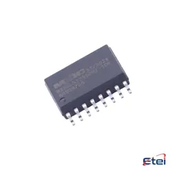
Images are for reference only
MAX2671EUT
+BOMUp-Down Converters
-
ManufacturerAnalog Devices / Maxim Integrated
-
Mfr. Part #MAX2671EUT
-
Datasheet MAX2671EUT DataSheet
-
In Stock11617
365 Days Quality Guarantee
7*24 hours service quarantee
90-day after-sales guarantee
Genuine Product Guarantee
Specifications
| Attribute | Value |
Overview
Description
With an integrated shutdown feature, the MAX2671EUT allows for power-saving when the amplifier is not in use. It typically operates with a supply voltage ranging from 2.7V to 5.5V, accommodating various power sources in electronic designs. The small SOT-23 package makes it suitable for compact designs, requiring minimal space on circuit boards.
The device is designed to improve the signal-to-noise ratio of weak input signals, ensuring clearer signal reception and better performance in challenging environmental conditions. With its low cost and efficient operation, the MAX2671EUT is widely used in personal navigation devices, smartphones, and other GPS-enabled systems.
Equivalent
Features
1. Frequency Range: Operates effectively in the 400MHz to 2.5GHz frequency range, making it versatile for various RF applications.
2. Low Noise Figure: Offers a low noise figure, which is essential for maintaining signal integrity by minimizing noise in the converted signal.
3. High-Linearity: Ensures excellent signal quality with high linearity, which is crucial for reducing distortion in high-performance systems.
4. Integrated LO Buffer: Contains an integrated local oscillator buffer that simplifies design and reduces the need for external components.
5. Single-Supply Operation: Operates with a single power supply, simplifying power management and integration into systems.
6. Small Package: Available in a compact SOT23-6 package, which is ideal for space-constrained applications.
7. Low Power Consumption: Designed for efficient power usage, making it suitable for battery-powered and portable devices.
These features make the MAX2671EUT suitable for various RF applications, including cellular base stations, cordless phones, and other wireless communication systems.
Pinout
1. RF IN: Input for the RF signal.
2. VCC: Power supply voltage input.
3. GND: Ground connection.
4. RF OUT: Output for the amplified RF signal.
5. SHDN (Shutdown): Logic input to enable or disable the amplifier.
6. BIAS: Bias connection for setting the operating point of the LNA.
This LNA is designed to offer low noise and high linearity, which is critical for enhancing weak GPS signals. The shutdown feature allows the device to save power when the LNA is not actively needed.