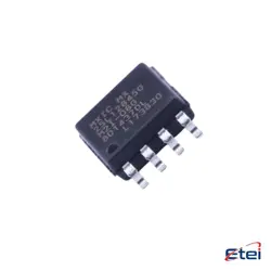
Images are for reference only
MC74F374DW
+BOMBUS DRIVER, F/FAST SERIES, 1-FUN
-
Manufactureronsemi
-
Mfr. Part #MC74F374DW
-
Datasheet MC74F374DW DataSheet
-
In Stock6403
365 Days Quality Guarantee
7*24 hours service quarantee
90-day after-sales guarantee
Genuine Product Guarantee
Specifications
| Attribute | Value |
| Package | Bulk |
| ProductStatus | Active |
Overview
Description
Packaged in a 20-pin SOIC (Small Outline Integrated Circuit), the MC74F374DW is compact, making it suitable for space-constrained applications. It operates typically at a supply voltage of 5V and supports TTL logic levels. The device is widely used in computing systems, digital systems, and communication devices for register and buffer functions. Its high-speed operation and reliable performance make it a popular choice in various industrial and consumer electronics.
Equivalent
Features
1. Octal D-Type Flip-Flop: The device contains eight flip-flops, allowing for simultaneous storage of eight bits of data.
2. 3-State Outputs: It supports 3-state outputs, enabling connection to a common bus line without interference when not selected.
3. Positive-Edge Triggered: Data is latched on the rising edge of the clock pulse, ensuring precise timing control.
4. High-Speed Operation: Part of the FAST (Fairchild Advanced Schottky TTL) series, it is designed for high-speed performance.
5. TTL Compatible: The inputs and outputs are compatible with TTL logic levels, making it suitable for integration into various TTL-based systems.
6. Supply Voltage: Typically operates at a standard TTL supply voltage of 5V.
7. Integrated Circuit Package: Available in a small surface-mount package (DW suffix indicates SOIC).
These features make the MC74F374DW suitable for applications requiring fast data storage and retrieval, such as microprocessor memory interfaces and data buffering.
Pinout
The MC74F374DW comes in a 20-pin SOIC (Small Outline Integrated Circuit) package. Here is a brief outline of the pin functions:
- Pins 1, 2, 3, 4, 5, 6, 7, 8: These are the data inputs (D0 to D7) for each of the eight flip-flops.
- Pin 9: This is the clock input (CP) that triggers the data transfer.
- Pin 10: Ground (GND).
- Pins 11, 12, 13, 14, 15, 16, 17, 18: These are the data outputs (Q0 to Q7) for each flip-flop.
- Pin 19: Output Enable (OE), active low.
- Pin 20: VCC (Power Supply).
The MC74F374DW is commonly used for data latching and storage applications in digital systems.