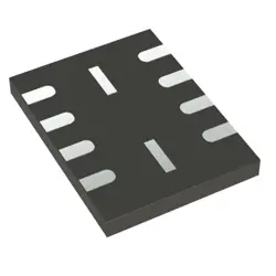
Images are for reference only
PCA9517ADP
+BOMInterface - Signal Buffers, Repeaters Bus buffer
-
ManufacturerNXP Semiconductors
-
Mfr. Part #PCA9517ADP
-
Datasheet PCA9517ADP DataSheet
-
In Stock8605
365 Days Quality Guarantee
7*24 hours service quarantee
90-day after-sales guarantee
Genuine Product Guarantee
Specifications
| Attribute | Value |
Overview
Description
Key features of the PCA9517ADP include its ability to isolate capacitance, allowing more devices on the I²C bus without degrading signal integrity, and its open-drain architecture, which ensures that it only drives the bus lines low to avoid conflicts. The device supports levels ranging from 2.3V to 5.5V on both sides, providing flexibility in system design. Moreover, it includes a rise-time accelerator, enhancing the performance of the bus lines.
The PCA9517ADP is typically used in applications like consumer electronics, communications systems, and embedded systems where different voltage domains are present.
Equivalent
1. TCA9517 by Texas Instruments - Offers similar functionality with level shifting capabilities for I2C signals.
2. PCA9515A by NXP - Another I2C bus repeater with similar characteristics.
3. LTC4311 by Analog Devices - Provides rise time acceleration and level shifting for I2C buses.
Ensure compatibility with your specific requirements before substituting components.
Features
1. Voltage-Level Translation: Supports level shifting between 1.0 V to 5.5 V VCCA and 1.8 V to 5.5 V VCCB, catering to different voltage nodes.
2. Dual Open-Drain I2C/SMBus: Facilitates communication between multiple I2C devices.
3. Bus Buffering: Provides buffering to extend bus capacitance and improve signal integrity in large and complex networks.
4. Rise Time Accelerator: Enhances signal rise times for improved data transfer reliability.
5. Enable Pin: Features an enable pin for enabling or disabling the buffer function, providing control over the buffer operation.
6. Clock Stretching and Arbitration: Supports clock stretching and arbitration, ensuring compatibility with standard I2C operations.
7. Hot Swap Capability: Allows devices to be connected or disconnected without disrupting the system, enhancing flexibility in dynamic environments.
8. Low Propagation Delay: Ensures timely data communication across the buffer.
9. ESD Protection: Equipped with electrostatic discharge protection for robust operation in various environments.
These features make it suitable for applications requiring reliable I2C signal buffering and level translation.
Pinout
The PCA9517ADP comes in a TSSOP (Thin Shrink Small Outline Package) package and typically has 8 pins. Here is a concise pin function description:
1. VCC(A): Supply voltage for the A-side, which can be lower than VCC(B).
2. SDAA: Serial Data line for the A-side.
3. SCLA: Serial Clock line for the A-side.
4. GND: Ground reference for the device.
5. SCLB: Serial Clock line for the B-side.
6. SDAB: Serial Data line for the B-side.
7. VCC(B): Supply voltage for the B-side, which is the higher voltage side.
8. EN: Enable pin to activate the repeater function.
The PCA9517ADP is used to ensure reliable communication between devices operating at different voltage levels by buffering and level shifting the I2C signals.
Manufacturer
Application
1. Consumer Electronics: Facilitates communication between microcontrollers and various peripherals like sensors and displays.
2. Computing Systems: Enhances data transfer between system management buses and monitoring components.
3. Automotive: Supports robust data exchange in vehicular control systems and infotainment units.
4. Industrial Automation: Improves communication reliability between different control modules and sensors.
5. Medical Devices: Ensures reliable data communication in equipment like diagnostic and monitoring devices.
By providing level shifting and buffering, it enhances signal integrity and supports communication over longer distances.