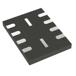
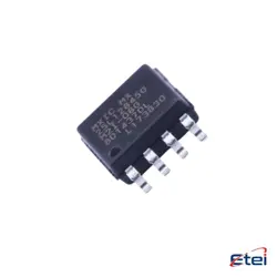
Images are for reference only
SN10501DBVR
+BOMIC AMP VOLTAGE FEEDBACK SOT23-5
-
ManufacturerTexas Instruments
-
Mfr. Part #SN10501DBVR
-
Datasheet SN10501DBVR DataSheet
-
In Stock4773
365 Days Quality Guarantee
7*24 hours service quarantee
90-day after-sales guarantee
Genuine Product Guarantee
Specifications
| Attribute | Value |
| Part Status | Active |
| Applications | Voltage Feedback |
| Output Type | Rail-to-Rail |
| Number of Circuits | 1 |
| -3db Bandwidth | 170 MHz |
| Slew Rate | 900V/µs |
| Current - Supply | 14 mA |
| Current - Output / Channel | 100 mA |
| Voltage - Supply, Single/Dual (±) | 2.7V ~ 16V, ±1.35V ~ 8V |
| Mounting Type | Surface Mount |
| Package / Case | SC-74A, SOT-753 |
| Supplier Device Package | SOT-23-5 |
| Base Product Number | SN10501 |
Overview
Description
The SN10501DBVR features a bi-directional level shifting capability, allowing signals to be translated in both directions. It supports high-speed operation, which is essential for applications like I2C and SPI communications. The package type is a small, surface-mounted Dual-In-Line Package (DIP), making it suitable for compact circuit designs.
Key specifications include low propagation delay, low power consumption, and robust noise immunity. This IC is commonly used in consumer electronics, automotive applications, and industrial systems where reliable voltage translation is critical. Overall, the SN10501DBVR plays a vital role in ensuring compatibility between different electronic components in modern devices.
Equivalent
1. TL431 (adjustable shunt voltage reference)
2. LM4040 (series voltage reference)
3. AD580 (precision voltage reference)
4. LT1009 (low drift voltage reference)
Always verify specifications and pin configurations to ensure compatibility for your specific application.
Features
1. Dual Buffers/Drivers: It contains two independent, high-speed, low-power buffers/drivers that can drive capacitive loads.
2. High-Speed Operation: Capable of operating at speeds up to 100 MHz.
3. Low Power Consumption: Designed for low quiescent current, making it suitable for battery-operated devices.
4. Output Drive Capability: Can drive up to 15 pF load at 2 V output swing.
5. Logic Compatibility: Compatible with TTL and CMOS logic levels.
6. Wide Supply Voltage Range: Operates with a supply voltage range of 3 V to 15 V.
7. Thermal Shutdown Protection: Built-in thermal shutdown feature for enhanced reliability.
8. Small Package Size: Offered in a compact SOIC-8 package, ideal for space-constrained applications.
These features make the SN10501DBVR suitable for various applications, including signal buffering and level shifting in digital circuits.
Pinout
Pin Functions:
1. Pin 1 (Offset Null): Adjusts the offset voltage.
2. Pin 2 (Inverting Input): The input where the signal is applied for inversion.
3. Pin 3 (Non-Inverting Input): The input for the non-inverted signal.
4. Pin 4 (V- or GND): Negative power supply or ground.
5. Pin 5 (Output): The output where the amplified signal is taken.
6. Pin 6 (V+ or Vcc): Positive power supply.
7. Pin 7 (NC): No connection.
8. Pin 8 (Offset Null): For offset adjustment, similar function as Pin 1.
This op-amp is designed for precision applications, providing features like low noise and high gain.
Manufacturer
Application
1. Consumer Electronics: Powering devices such as smartphones, tablets, and laptops.
2. Telecommunications: Supporting wireless and networking equipment.
3. Industrial Automation: Providing stable power for sensors and controllers.
4. Automotive: Used in infotainment systems and other electronic control units.
5. Medical Devices: Ensuring reliable power for medical instrumentation.
Its features include low noise, high precision, and thermal protection, making it suitable for applications requiring stable and efficient power management.