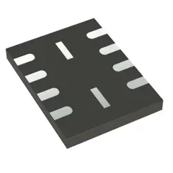
Images are for reference only
SN74LVC8T245DBR
+BOMIC TRANSLATION TXRX 5.5V 24SSOP
-
ManufacturerTexas Instruments
-
Mfr. Part #SN74LVC8T245DBR
-
Datasheet SN74LVC8T245DBR DataSheet
-
Package SSOP-24
-
In Stock4255
365 Days Quality Guarantee
7*24 hours service quarantee
90-day after-sales guarantee
Genuine Product Guarantee
Specifications
| Attribute | Value |
| Package / Case | Tape & Reel (TR),Cut Tape (CT) |
| Series | 74LVC |
| Part Status | Active |
| Logic Type | Translation Transceiver |
| Number of Elements | 2 |
| Number of Bits per Element | 8 |
| Output Type | 3-State |
| Current - Output High Low | 32mA, 32mA |
| Voltage - Supply | 1.65V ~ 5.5V |
| Operating Temperature | -40°C ~ 85°C (TA) |
| Mounting Type | Surface Mount |
Overview
Description
Key features include direction control, a 3-state output for bus-oriented applications, and the ability to withstand higher-voltages with its Ioff circuitry, preventing backflow current when the device is powered down. The SN74LVC8T245DBR is packaged in a small-outline integrated circuit (SOIC) and is suited for various applications, such as portable electronics, computing, and networking. Its robust design and flexibility in voltage translation make it a versatile choice for designers needing reliable data transfer between different logic levels.
Equivalent
Features
1. Voltage Level Shifting: Operates with two separate power-supply rails, allowing bidirectional voltage level translation between 1.4 V and 3.6 V on A-port and 1.65 V to 5.5 V on B-port.
2. High-Speed Operation: Ensures efficient data transfer with a maximum data rate up to 380 Mbps.
3. OE and DIR Control: Features output-enable (OE) and direction-control (DIR) pins for easily managing the data flow between buses.
4. Low Power Consumption: Includes a partial power-down mode for power savings.
5. Ioff Support: Prevents backflow of current, which safeguards the device during partial power-down conditions.
6. Wide Operating Temperature Range: Suitable for industrial applications, operating from -40°C to 85°C.
7. Robust Design: Features overvoltage-tolerant inputs and outputs up to 5.5 V.
8. Compact Package: Available in a TSSOP package for space-constrained applications.
These features make it suitable for interfacing mixed-voltage systems, ensuring flexibility and efficiency in complex electronic applications.
Pinout
Key functions include:
- Bidirectional Data Transfer: It allows for data transmission in both directions between buses A and B. The direction is controlled by the DIR pin.
- Output Enable: The OE pin is used to enable or disable the outputs, placing them in a high-impedance state when disabled.
- Level Shifting: It provides voltage level translation between the two buses.
The typical pin configuration includes power supply pins (VCCA and VCCB), ground pins (GND), input/output pins for the A and B buses, and control pins (DIR and OE). This makes it suitable for applications where voltage translation and bidirectional data flow are needed.