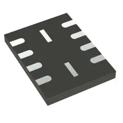
Images are for reference only
SNJ54LS157J
+BOM-
ManufacturerTexas Instruments
-
Mfr. Part #SNJ54LS157J
-
In Stock8198
365 Days Quality Guarantee
7*24 hours service quarantee
90-day after-sales guarantee
Genuine Product Guarantee
Specifications
| Attribute | Value |
| Shipping Restrictions | Mouser does not presently sell this product in your region. |
| Mounting Type | Through Hole |
| Package / Case | CDIP-16 |
| Supply Voltage - Min | 4.5 V |
| Supply Voltage - Max | 5.5 V |
| Minimum Operating Temperature | - 55 C |
| Maximum Operating Temperature | + 125 C |
| Brand | Texas Instruments |
| Product | Selectors / Multiplexers |
| Product Type | Encoders, Decoders, Multiplexers & Demultiplexers |
| Factory Pack Quantity | 1 |
| Subcategory | Logic ICs |
| Operating Supply Voltage | 5 V |
| Width | 6.92 mm |
| Height | 4.57 mm |
| Technology | Bipolar |
| Logic Family | LS |
| Number of Input Lines | 2 Input |
| Number of Output Lines | 1 Output |
| Propagation Delay Time | 14 ns at 5 V |
| Function | Multiplexer |
| Length | 19.56 mm |
| Logic Type | Data Selectors/Multiplexers |
| Series | SN54LS157 |
| Packaging | Tube |
| High Level Output Current | - 400 uA |
| Low Level Output Current | 4 mA |
| Number of Circuits | 4 Circuit |
Overview
Description
The SNJ54LS157J is a quad 2-input multiplexer, designed for high-speed digital applications. It operates in the military temperature range and complies with the standards for the military version of the 7400 series logic devices. The device features four independent 2-input multiplexers, allowing for the selection of one of two data inputs through a common select line, thus facilitating data routing in complex circuits.
Each multiplexer has two data inputs (A and B) and one output (Y). The selection is controlled by a single select line (S). When S is low, the output Y reflects input A; when S is high, Y reflects input B. The SNJ54LS157J is characterized by low power consumption and high-speed operation, making it suitable for various applications in communication systems, automotive electronics, and military devices.
In summary, the SNJ54LS157J is a versatile component for efficient signal management in digital circuits, ideal for environments requiring robust performance and reliability.
Each multiplexer has two data inputs (A and B) and one output (Y). The selection is controlled by a single select line (S). When S is low, the output Y reflects input A; when S is high, Y reflects input B. The SNJ54LS157J is characterized by low power consumption and high-speed operation, making it suitable for various applications in communication systems, automotive electronics, and military devices.
In summary, the SNJ54LS157J is a versatile component for efficient signal management in digital circuits, ideal for environments requiring robust performance and reliability.
Equivalent
The SNJ54LS157J is a quad 2-input multiplexer. Equivalent products include the SN74LS157, SN74ALS157, and MC74LS157. Other compatible options may include the 74HC157 and 74HCT157, which are high-speed CMOS versions. Always check specific datasheets for detailed pin configurations and specifications to ensure compatibility for your application.
Features
The SNJ54LS157J is a high-speed quad 2-input multiplexer, designed for military applications with enhanced reliability. Key features include:
1. Quad 2-Input Multiplexer: Contains four independent multiplexers, allowing selection between two data sources for each channel.
2. High-Speed Operation: Designed for fast switching, with propagation delays typically around 10 ns, enabling rapid data processing.
3. Wide Supply Voltage Range: Operates on a supply voltage range of 4.5V to 5.5V, compatible with various logic levels.
4. Low Power Consumption: Consumes minimal power, making it suitable for battery-operated devices.
5. TTL Compatible: Compatible with TTL logic levels, allowing integration into existing systems.
6. Temperature Range: Rated for operation in extended temperature ranges, suitable for harsh environments.
7. Pin Configuration: Available in a 16-pin dual in-line package (DIP), facilitating easy integration into circuits.
These features make the SNJ54LS157J ideal for applications requiring reliable and fast data routing in demanding environments.
1. Quad 2-Input Multiplexer: Contains four independent multiplexers, allowing selection between two data sources for each channel.
2. High-Speed Operation: Designed for fast switching, with propagation delays typically around 10 ns, enabling rapid data processing.
3. Wide Supply Voltage Range: Operates on a supply voltage range of 4.5V to 5.5V, compatible with various logic levels.
4. Low Power Consumption: Consumes minimal power, making it suitable for battery-operated devices.
5. TTL Compatible: Compatible with TTL logic levels, allowing integration into existing systems.
6. Temperature Range: Rated for operation in extended temperature ranges, suitable for harsh environments.
7. Pin Configuration: Available in a 16-pin dual in-line package (DIP), facilitating easy integration into circuits.
These features make the SNJ54LS157J ideal for applications requiring reliable and fast data routing in demanding environments.
Pinout
The SNJ54LS157J is a quad 2-input multiplexer/demultiplexer with a total of 16 pins. Its primary function is to select one of several input lines and route it to a single output line based on the select inputs.
Pin Configuration:
1. 1-4: Inputs A0, A1, B0, B1
2. 5: Enable (G)
3. 6-9: Outputs Y0, Y1, Y2, Y3
4. 10-12: Inputs C0, C1, D0, D1
5. 13: Ground (VSS)
6. 14: VCC (Power Supply)
7. 15-16: Select inputs S0, S1
The device allows for the selection of one of four data inputs to be sent to the output based on the select lines (S0 and S1) and can enable or disable output based on the G pin. It operates at high speed and is suitable for various digital applications.
Pin Configuration:
1. 1-4: Inputs A0, A1, B0, B1
2. 5: Enable (G)
3. 6-9: Outputs Y0, Y1, Y2, Y3
4. 10-12: Inputs C0, C1, D0, D1
5. 13: Ground (VSS)
6. 14: VCC (Power Supply)
7. 15-16: Select inputs S0, S1
The device allows for the selection of one of four data inputs to be sent to the output based on the select lines (S0 and S1) and can enable or disable output based on the G pin. It operates at high speed and is suitable for various digital applications.
Manufacturer
The SNJ54LS157J is manufactured by Texas Instruments (TI), a leading semiconductor company based in the United States. Founded in 1930, Texas Instruments specializes in designing and manufacturing a wide range of electronics, including analog and digital semiconductors, embedded processors, and integrated circuits. The company is well-known for its innovations in various technologies, serving diverse industries such as telecommunications, automotive, consumer electronics, and industrial applications. TI also produces calculators and digital signal processing (DSP) solutions, making it a key player in the global electronics market.
Application
The SNJ54LS157J is a quad 2-input multiplexer designed for high-speed digital logic applications. Its primary application areas include data routing, signal selection, and system control in telecommunications, computer systems, and embedded systems. It can be used in applications requiring logic functions such as data multiplexing, demultiplexing, and bus switching. Additionally, it finds use in digital signal processing, automatic test equipment, and industrial automation, where efficient data management and routing are essential. Its military-grade specification also makes it suitable for aerospace and defense applications.
Package
The SNJ54LS157J is packaged in a dual in-line package (DIP), specifically a 14-pin configuration. It is designed for military applications with enhanced performance and reliability.