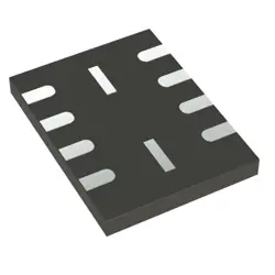
Images are for reference only
ADCMP605BCPZ
+BOM-
ManufacturerAnalog Devices
-
Mfr. Part #ADCMP605BCPZ
-
In Stock9405
365 Days Quality Guarantee
7*24 hours service quarantee
90-day after-sales guarantee
Genuine Product Guarantee
Specifications
| Attribute | Value |
| Brand | Analog Devices |
| Packaging | Reel |
| Factory Pack Quantity | 1500 |
Overview
Description
The ADCMP605BCPZ is a high-speed, low-power comparator designed for precision applications. It features a rail-to-rail input and output, allowing it to handle signals that extend to the supply voltage limits, making it versatile for various circuits. The device operates from a supply voltage range of 2.7V to 5.5V and offers a propagation delay of approximately 12 ns, enabling fast signal processing.
With a low input bias current, it minimizes loading effects on the preceding stages, ensuring accurate signal detection. The comparator has a high gain bandwidth product, making it suitable for high-frequency applications. Additionally, the ADCMP605BCPZ includes built-in hysteresis to improve noise immunity and reduce false triggering.
It is available in a compact 8-lead LFCSP package, making it ideal for space-constrained designs. This comparator is commonly used in applications like data acquisition systems, signal processing, and zero-crossing detection. Overall, the ADCMP605BCPZ combines performance and efficiency, making it a reliable choice for modern electronic designs.
With a low input bias current, it minimizes loading effects on the preceding stages, ensuring accurate signal detection. The comparator has a high gain bandwidth product, making it suitable for high-frequency applications. Additionally, the ADCMP605BCPZ includes built-in hysteresis to improve noise immunity and reduce false triggering.
It is available in a compact 8-lead LFCSP package, making it ideal for space-constrained designs. This comparator is commonly used in applications like data acquisition systems, signal processing, and zero-crossing detection. Overall, the ADCMP605BCPZ combines performance and efficiency, making it a reliable choice for modern electronic designs.
Equivalent
The ADCMP605BCPZ is a high-speed comparator. Equivalent products include the TLV3701, LM393 and the MAX9001. These comparators offer similar functionalities, such as fast response times and low power consumption. However, ensure to check specific electrical characteristics and package types for compatibility with your application.
Features
The ADCMP605BCPZ is a high-speed, low-power comparator designed for various applications. Key features include:
1. Input Voltage Range: The device operates with a supply voltage range of 2.7V to 5.5V, making it suitable for battery-operated devices.
2. Propagation Delay: It offers a fast response time with a propagation delay of approximately 3.5 ns, ensuring rapid signal processing.
3. Low Power Consumption: The comparator has a quiescent current of 1.2 mA, contributing to energy efficiency.
4. Output Type: The ADCMP605 features a push-pull output, allowing for direct interfacing with TTL/CMOS logic levels.
5. Hysteresis: Integrated hysteresis helps improve noise immunity and provides stable switching characteristics.
6. Temperature Range: It operates effectively in a wide temperature range from -40°C to +125°C, suitable for industrial and automotive environments.
7. Package Type: Available in a compact 8-lead LFCSP package, facilitating space-saving designs.
These features make the ADCMP605BCPZ ideal for applications in data acquisition, signal conditioning, and various electronic circuits.
1. Input Voltage Range: The device operates with a supply voltage range of 2.7V to 5.5V, making it suitable for battery-operated devices.
2. Propagation Delay: It offers a fast response time with a propagation delay of approximately 3.5 ns, ensuring rapid signal processing.
3. Low Power Consumption: The comparator has a quiescent current of 1.2 mA, contributing to energy efficiency.
4. Output Type: The ADCMP605 features a push-pull output, allowing for direct interfacing with TTL/CMOS logic levels.
5. Hysteresis: Integrated hysteresis helps improve noise immunity and provides stable switching characteristics.
6. Temperature Range: It operates effectively in a wide temperature range from -40°C to +125°C, suitable for industrial and automotive environments.
7. Package Type: Available in a compact 8-lead LFCSP package, facilitating space-saving designs.
These features make the ADCMP605BCPZ ideal for applications in data acquisition, signal conditioning, and various electronic circuits.
Pinout
The ADCMP605BCPZ is a high-speed, low-power comparator with an 8-pin configuration. Its pin count and functions are as follows:
1. V+ (Pin 1): Positive supply voltage.
2. IN+ (Pin 2): Non-inverting input.
3. IN- (Pin 3): Inverting input.
4. V- (Pin 4): Negative supply voltage or ground.
5. OUT (Pin 5): Comparator output.
6. GND (Pin 6): Ground reference for the device.
7. RFB (Pin 7): Feedback resistor pin (optional for hysteresis).
8. NC (Pin 8): No connect; can be left unconnected.
The ADCMP605BCPZ provides a fast response time and is designed for applications requiring precise signal comparisons, making it suitable for a variety of electronic circuits.
1. V+ (Pin 1): Positive supply voltage.
2. IN+ (Pin 2): Non-inverting input.
3. IN- (Pin 3): Inverting input.
4. V- (Pin 4): Negative supply voltage or ground.
5. OUT (Pin 5): Comparator output.
6. GND (Pin 6): Ground reference for the device.
7. RFB (Pin 7): Feedback resistor pin (optional for hysteresis).
8. NC (Pin 8): No connect; can be left unconnected.
The ADCMP605BCPZ provides a fast response time and is designed for applications requiring precise signal comparisons, making it suitable for a variety of electronic circuits.
Manufacturer
The ADCMP605BCPZ is manufactured by Analog Devices, Inc. Analog Devices is a multinational company known for its expertise in high-performance analog, mixed-signal, and digital signal processing technologies. Founded in 1965, the company specializes in providing a wide range of semiconductor solutions, including amplifiers, converters, sensors, and signal processing products, which are utilized in various applications such as communications, automotive, industrial automation, healthcare, and consumer electronics.
Analog Devices is recognized for its innovation and commitment to quality, serving a diverse market with a focus on precision and reliability. The ADCMP605BCPZ itself is a comparator designed for applications requiring high-speed performance and low power consumption, reflecting the company's dedication to advanced technology solutions. Overall, Analog Devices plays a crucial role in the development and advancement of electronic systems across various industries.
Analog Devices is recognized for its innovation and commitment to quality, serving a diverse market with a focus on precision and reliability. The ADCMP605BCPZ itself is a comparator designed for applications requiring high-speed performance and low power consumption, reflecting the company's dedication to advanced technology solutions. Overall, Analog Devices plays a crucial role in the development and advancement of electronic systems across various industries.
Application
The ADCMP605BCPZ is a high-speed comparator primarily used in applications requiring fast response times and low power consumption. Key application areas include:
1. Signal Conditioning: Optimizing signal levels in analog circuits.
2. Data Acquisition Systems: Enhancing the performance of ADCs.
3. Voltage Level Detection: Monitoring voltage levels in power management systems.
4. Pulse Width Modulation: Generating PWM signals for motor control.
5. Communication Systems: Enabling high-speed data transmission and signal integrity.
6. Transistor Switching Circuits: Driving transistors in digital logic and analog applications.
Its fast propagation delay and low offset voltage make it suitable for precision applications.
1. Signal Conditioning: Optimizing signal levels in analog circuits.
2. Data Acquisition Systems: Enhancing the performance of ADCs.
3. Voltage Level Detection: Monitoring voltage levels in power management systems.
4. Pulse Width Modulation: Generating PWM signals for motor control.
5. Communication Systems: Enabling high-speed data transmission and signal integrity.
6. Transistor Switching Circuits: Driving transistors in digital logic and analog applications.
Its fast propagation delay and low offset voltage make it suitable for precision applications.
Package
The ADCMP605BCPZ is packaged in a 5-lead SOT-23 package.